
Professor Yoshio Waseda – Understanding the Atomic Structure of New Materials
Materials science – the discovery and characterisation of new materials – drives forward the creation of new technology. In particular, the development of thin films of materials is vital to the electronics industry, as they are used in various device components such as displays and sensors. The properties of these materials are defined by their atomic structure, and until recently it was a major challenge for scientists to accurately characterise this. Towards this aim, Professor Yoshio Waseda and his team at the Institute of Multidisciplinary Research for Advanced Materials have developed a novel method for characterising the atomic structure of thin films.
Materials Science
The material world around us is changing rapidly. The discovery of new materials, or finding new ways to process and use existing materials, is what drives forward the creation of new technologies. From the discovery of metal alloys and rubber in the early 1800s, to the characterisation of graphene in 2004, scientists are discovering new materials all the time.
Materials scientists discover and design new materials that can be used across many different technologies. They hope to understand how the processing of a specific solid material can influence that material’s properties through alterations to its atomic structure.
Today’s materials research focuses on a wide range of areas, including ceramics, polymers and nanomaterials. The study and development of new materials is particularly important for the field of electronics. Many of our everyday electronic items, such as LCD televisions and mobile phones owe their evolution to innovative discoveries, including oxide semiconductors, composite plastics and strengthened glass.
For instance, the development of the smartphone as we know it would not have been possible without the invention of the liquid-crystal display and thin-film transistor (TFT). The field effect transistor (FET), a vital component of many computer devices, also comprises a thin-film semiconducting material and requires far less energy to operate than previous transistors, helping to meet society’s requirements for energy saving.
The arrangement and types of atoms in a material directly affects the material’s behaviour, such as its electronic properties. Therefore, scientists are always eager to find new ways to study atomic structure in detail, so that they can more effectively fine tune material properties. Towards this aim, Professor Yoshio Waseda and his colleagues at the Institute of Multidisciplinary Research for Advanced Materials in Japan have developed a novel method to study the atomic structure of thin films of materials.

Amorphous Materials
Materials are usually made of multiple types of atoms (different elements). By understanding how different combinations of elements create different physical properties, scientists can begin to simulate new materials to meet specific demands.
Scientists study the atomic arrangement by looking at how well ordered the constituent atoms or molecules are in a given material. They look at how regularly spaced neighbouring atoms or molecules are, as well as how random their distribution is across a wider area within a material. In crystalline solid materials, these units are very well ordered. Each atom or molecule has multiple neighbours that are equal distance from each other (an ordered atomic structure).
However, so-called ‘amorphous’ materials have a disordered atomic structure, with no repeating pattern. ‘In liquids and glass,’ describes Professor Waseda, ‘the atoms or molecules are distributed at random with little space between them.’ Professor Waseda’s research focus is to improve our understanding and make it easier to study the atomic structure of amorphous materials, particularly amorphous thin films (layers of material between a nanometre and several micrometres thick). Thin films often possess unique properties that make them ideal for many device applications, including integrated circuits.
Thin films play a vital role in modern technology that we as consumers often take for granted, which is their role as semiconductors. Semiconductors form the basis of our modern electronic devices, where they perform vital functions. Currently, the most common semiconducting material used in our electronic devices and solar cells is silicon. The ability to measure the atomic structure of alternative types of semiconductors allows material scientists to design new semiconducting materials for specific uses, such as high-performing thin films for next generation electronic devices.
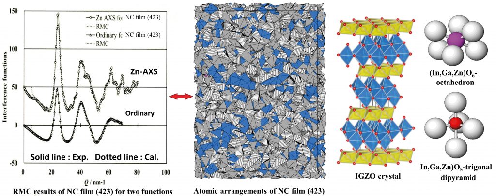
Figure 1. RMC results reproduce two structural functions independently obtained from measurement. Note that 423 is the ratio of In²O³, Ga²O³ and ZnO.
X-Ray Scattering Techniques
Studying the atomic structure of an amorphous material is a challenge, as the atoms or molecules are randomly distributed with no regular, recurring pattern. In order to study the atomic structure of amorphous thin film materials, Professor Waseda and his team combined x-ray scattering techniques with mathematical models.
X-ray scattering is a non-destructive method of analysing a material. When an x-ray beam hits a sample of material, it is scattered (absorbed and re-emitted in different directions) by individual atoms or molecules in the material. Scientists can study the intensity and patterning to this scatter to determine the atomic structure and other properties of thin films.
The team used a technique called x-ray scattering for obtaining the ‘radial distribution function’ of the material. The radial distribution function describes the probability of finding atoms within a specified volume and within a particular distance of each other. In addition, the local environmental structure around a specific element is required for describing the structure of an amorphous material. For this purpose, the team also employed anomalous x-ray scattering combined with a simulation technique called Reverse Monte Carlo. Anomalous x-ray scattering is known to be useful for both crystalline and non-crystalline materials for studies of surface and bulk materials.
The team’s method has been successfully used to characterise the structures of thin films that are less than a micrometre thick, and can be applied to both crystalline and amorphous materials. This has provided a new in-depth look at the properties of these materials.

Figure 2. Atomic-scale structural model for reproducing two independent structural functions. Cross-hatched pattern: oxygen-polyhedral units around In; grey: oxygen-polyhedral units around Zn; blue: oxygen-polyhedral units around Ga.
IGZO Films
In their recent work, Professor Waseda and his team have been investigating the structural properties of a particular material called indium gallium zinc oxide (IGZO), which is a semiconducting material. Thin films of IGZO are already in use in a variety of electronic devices. For example, IGZO thin films can be found in flat panel displays, such as smartphone screens and tablet displays, as they have an improved power consumption rate compared to other thin films, providing energy-saving features.
There are multiple types of IGZO film, including a nanocrystalline film and a newly discovered crystalline film (CAAC IGZO film). These both show features that imply their structure includes individual crystals, indicating that there could be some order within their structures. However, scientists had not yet fully elucidated the discrete crystal structures within these films. Professor Waseda and his colleagues have been investigating their structure to better understand their physical and chemical properties.
Using their anomalous x-ray scattering method, the team investigated the ‘anomalous dispersion effect’ of an element of interest by tuning the incidence x-ray energy to collect data on the atomic structure of that specific element in the thin film. They also combined this data with simulations to create an atomic-scale model for the IGZO films. Their aim was to gain the atomic arrangements in order to independently reproduce two structural functions obtained from measurement (see Fig. 1).
The team initially discovered that there was a distinct crystalline feature within the NC (nanocrystalline) and CAAC films (see Fig. 2). It was previously thought that IGZO films were structured in layers, with slabs of indium and oxygen alternating with slabs of zinc, gallium and oxide molecules. The team found that the four elements are basically mixed together to form crystalline clusters in both types of film, each of which exhibits the characteristic layered-structure of IGZO (see Fig. 3).
The team refer to this structure comprising nanometre-sized structural features as a crystalline-cluster-composite (triple C) system. This atomic arrangement of nanometre-sized crystalline clusters contributes to the resilience of this material against atomic rearrangement, even when the structure has a relatively high density. Such features are promising for the production of large square films, while also benefiting the production of IGZO films with sufficient reliability for device fabrication in microelectronics.
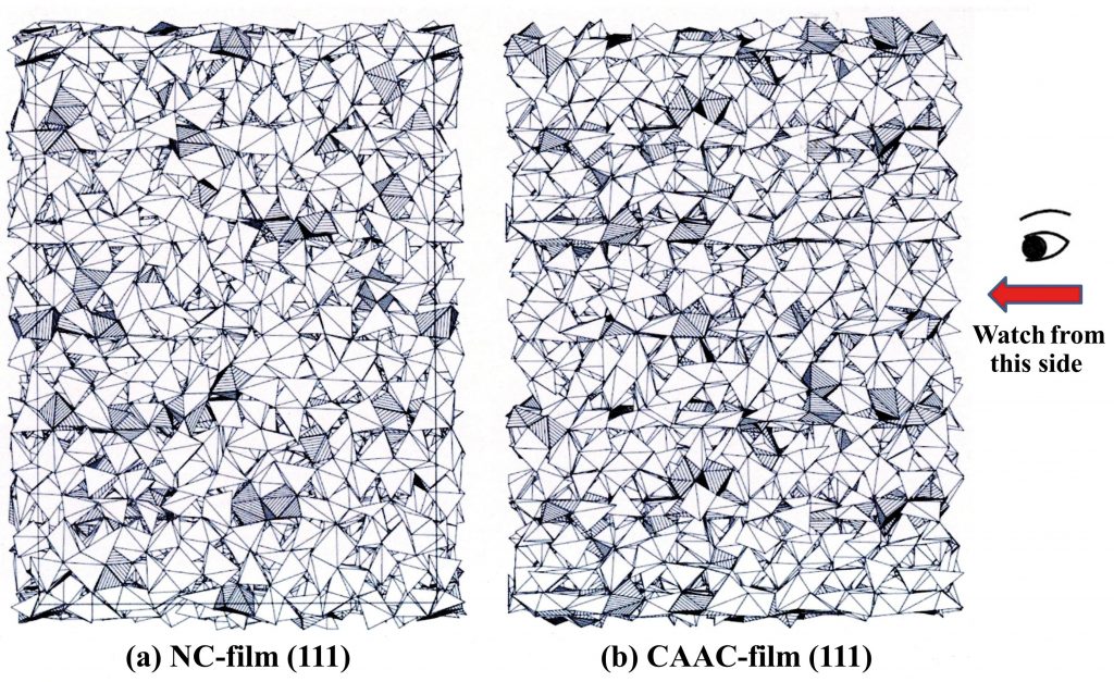
Figure 3. When focusing on the atomic coordination state only using the same model without colour coding, the residual crystalline clusters attributed to the particular layered structure of IGZO are detected in both films, particularly when observed from the side.
The Future of Materials Science
This combination of gathering data from laboratory analysis techniques along with modelling atomic structures is an important aspect of materials science research. Material scientists hope to fully characterise materials that are already in use to understand how their atomic structure relates to their physical properties, such as their ability to conduct electricity or how brittle they are under certain conditions. Once scientists can determine exactly how different chemical combinations produce these properties, they can easily simulate a material with those required properties.
In a world of rapidly developing technology, it is vital we fully understand the properties of new materials to ensure we can get the maximum value from each exciting discovery. Professor Waseda’s x-ray scattering technique to accurately model the atomic structure will play a vital role moving forward. As a non-invasive, non-destructive technique that can be applied to a wide variety of material types, it will be invaluable to understanding the chemical, electrical and magnetic properties of both existing and yet-to-be discovered materials.
Reference
https://doi.org/10.33548/SCIENTIA447
Meet the researcher

Professor Yoshio Waseda
Emeritus Professor of Tohoku University
Founding Director of the Institute of Multidisciplinary Research for Advanced Materials
Tohoku University
Sendai
Japan
Professor Yoshio Waseda is a materials scientist based at Tohoku University in Sendai, Japan. He is particularly interested in the structure of non-crystalline materials, and his long research career has led to over 700 publications. After completing his PhD in Materials Science at Tohoku University in 1973, he went on to lecture there, interspersed with some time at the University of Toronto and the University of Pennsylvania. Professor Waseda founded the Institute for Advanced Materials Processing in 1993 and the Institute of Multidisciplinary Research for Advanced Materials in 2001, and is currently Director of the Institute of Electromagnetic Materials. He has been the recipient of many awards such as TMS Leadership award and Honda Memorial Gold Metal award, and was most recently awarded The Order of the Sacred Treasure from the Emperor of Japan. Professor Waseda also holds five patents, and regularly collaborates with industry.
CONTACT
E: yoshio.waseda.d7@tohoku.ac.jp
W: http://www2.tagen.tohoku.ac.jp/en/index.html
W: http://www.imr.tohoku.ac.jp/en/about/divisions-andcenters/research-division/15.html
KEY COLLABORATORS
Professor Kazumasa Sugiyama, Institute for Materials Research, Tohoku University
Professor Shigeru Suzuki, Institute of Multidisciplinary Research for Advanced Materials
Dr Toru Kawamata, Institute for Materials Research, Tohoku University
Dr Shunpei Yamazaki, Semiconductor Energy Laboratory Co. Ltd.
FURTHER READING
Y Waseda, K Sugiyama & T Kawamata, Nanometer-sized crystalline clusters of IGZO films determined from the grazing incidence x-ray scattering and anomalous x-ray scattering data combined with reverse Monte Carlo simulations, Materials Transactions, 2018, 59, 11.
S Yamazaki & T Tsutsui (editors), Physics and Technology of Crystalline Oxide Semiconductors- CAAC-IGZO Application to Displays, John Wiley & Sons, West Sussex, 2017, ISBN: 9781119247456.
Y Waseda, S Suzuki & M Saito, A new method of materials characterization for a complex system by obtaining the middle range ordering, High Temperature Materials and Processing, 2005, 23, 1.
Y Waseda, Anomalous X-ray Scattering for Materials Characterization -Atomic Scale Structure Determination, Springer-Verlag, Heidelberg, 2002, ISBN: 3-540-43443-7.
Creative Commons Licence
(CC BY 4.0)
This work is licensed under a Creative Commons Attribution 4.0 International License. 
What does this mean?
Share: You can copy and redistribute the material in any medium or format
Adapt: You can change, and build upon the material for any purpose, even commercially.
Credit: You must give appropriate credit, provide a link to the license, and indicate if changes were made.
More articles you may like

Grandmothers: Innovation Through Tradition
Grandmother Project – Change through Culture (GMP) is an organisation dedicated to documenting the role of grandmothers and demonstrating the effectiveness of grandmother-inclusive strategies in improving the health and well-being of women, children, and adolescents. GMP’s groundbreaking work challenges conventional wisdom to transform community-based interventions in Africa and beyond, harnessing a powerful but often overlooked resource: the wisdom and influence of grandmothers.

Dr Robert Larkin | Cultivating Change to Improve Soil Health and Increase Potato Yield
Environmental quality and food production are facing the pressing challenges of climate change and global population growth. Dr Robert Larkin from the United States Department of Agriculture-Agricultural Research Service (USDA-ARS) and a team of plant scientists developed and tested a range of crop management systems to help overcome these compounding challenges. Their work is improving soil health and increasing the yield of potato crops, contributing to the future food security of nations.

Professor Giorgio Buttazzo | Artificial Intelligence and a Crossroads for Humanity
Where do we stand with artificial intelligence? Might machines take over our jobs? Can machines become conscious? Might we be harmed by robots? What is the future of humanity? Professor Giorgio Buttazzo of Scuola Superiore Sant’Anna is an expert in artificial intelligence and neural networks. In a recent publication, he provides considered insights into some of the most pressing questions surrounding artificial intelligence and humanity.

Dr Ralf Adam | New Technologies Shaping the Future of Oral Hygiene
Understanding the efficiency of various toothbrush technologies is essential for achieving optimal oral health. Dr Ralf Adam, who leads a dedicated team at Procter & Gamble in Germany, is keen to investigate the complexities of these technologies. His team have provided new insights into the best toothbrush types for plaque removal and the maintenance of gum health. By highlighting the importance of informed oral care decisions and ongoing investigations, this vital research works towards ensuring everyone can achieve a brighter, healthier smile.