
Wolfspeed & International Femtoscience: Creating a New Generation of Capacitors
Capacitors are a vital component in virtually every electronic device we use, and yet, innovations that make them more efficient have been a long time coming. Mr John Fraley and his colleagues at Wolfspeed, A Cree Company, and International Femtoscience are now working on a new generation of capacitors, which they believe could offer vast improvements over current technologies. They have developed a process they hope will greatly improve the energy storage capabilities of capacitors, satisfying what has become a desperate market need.
As the world of technology advances faster than ever before, researchers at Wolfspeed and International Femtoscience believe that one type of material will ensure that the capabilities of electrical components can keep up: the wide bandgap semiconductor.
Semiconductors are instrumental in electronic systems. Essentially acting as a cross between an insulator and a conductor, they are composed of materials that can be controlled to resist electrical current to varying degrees. ‘Wide bandgap’ semiconductors have structural properties that make them more resistant to electrical currents than regular semiconductors, allowing them to operate at extremely high voltages.
Mr Fraley and his colleagues at Wolfspeed and International Femtoscience believe that constructing wide bandgap semiconductors with the highest possible quality materials is a key enabling technology for next generation electronics in general, and power electronics especially.
 Their materials of choice are silicon carbide (SiC) and gallium nitride (GaN). By fabricating semiconductors from these compounds, Wolfspeed and International Femtoscience aim to improve the performance of electrical circuits in a wide array of devices. In doing so, the companies have become well acquainted with an array of techniques in fabricating materials with highly desirable electrical properties. They have now focused their attention on using their expertise to innovate one of the most ubiquitous components in electronics: the humble capacitor.
The Champion of Electronic Circuits
Capacitors can vary wildly in construction and physical form. Most capacitors contain at least two electrical conductors which are separated by an electrical insulator. The combination conductor-insulator-conductor ‘sandwich’ then constitutes a two-terminal device that stores potential energy in an electric field. This electric field will result in a net positive charge on one conductor and a net negative charge on the other conductor.
After the capacitor is charged in this way, the electrons in the negatively-charged plate want to move back to their natural position – creating a current in the circuit that flows in the opposite direction to the one that was originally induced. This effect is incredibly useful, as it allows energy to be stored in the capacitor until it is needed.
More sophisticated capacitors introduce a ‘dielectric’ material between the two plates. Common dielectric materials include glass, ceramic, plastic film, paper, mica, and oxide materials. The electric field that exists across the plates causes the material to become ‘polarised’ – in effect meaning it attracts the electrons in the negatively-charged plate while pushing them away from the positively-charged plate.
E-book

Audio-book

Reference
https://doi.org/10.26320/SCIENTIA246
Share
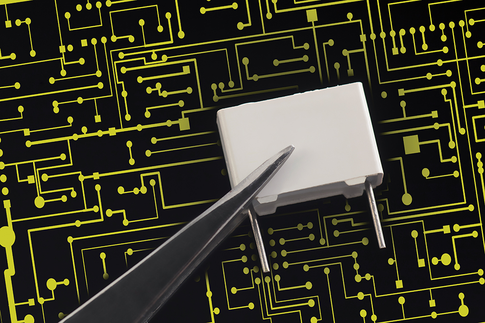
Capacitors have a wide array of uses in electronic systems. Capacitors are utilised to store energy, so that they act like temporary batteries or other types of rechargeable energy storage systems. They are used widely in power and signal processing to make filters that can discriminate between different frequencies of electrical current. They can be used to represent information by the energy stored within them. For the researchers at Wolfspeed and International Femtoscience, capacitors are critical components in their wide bandgap-based power module systems. However, current capacitor technology requires a large volume to achieve the appropriate voltage ratings for some of their high-voltage power conversion systems.
Long Awaited Advances
Mr Fraley believes that the much-anticipated improvements in dielectric materials can be realised through fabricating parallel plate capacitors utilising thin layers of diamond sandwiched between layers of a titanium-tungsten alloy, and stacking them on top of each other. As the Wolfspeed and International Femtoscience researchers describe in a report, diamond has ‘exceptional physical and electrical qualities’, in that remarkably high voltages can be blocked by it, allowing it to store a lot of energy. Stacking thin layers of such ‘metallised’ diamond would allow for very high voltage and high capacitance density components that enable highly efficient SiC power electronic systems.
The first steps taken by Mr Fraley and his colleagues in designing their new generation of capacitors were to devise a method for fabricating ultra-thin layers of exceptionally high-quality diamond. They decided on the method of ‘chemical vapour deposition’ (CVD), a process that involves exposing a surface to vaporised particles, and these particles are then deposited onto the surface as thin films. CVD is commonly used by Wolfspeed and International Femtoscience to procure high-quality semiconductors for a variety of purposes, giving the team the knowledge they need to plan the method.
The next challenge was to figure out the best possible stacking arrangement of diamond layers – a configuration that would allow for the strongest bonding between the layers. The researchers also needed to determine the precise atomic structure of diamond that would give rise to the most useful dielectric properties of the overall capacitor. Finally, they would need to test prototypes of their capacitors – determining the limitations of the early models, which would help them to optimise the dielectric properties of their capacitors in subsequent models.
Initiating Stack-up
To procure each stack, Mr Fraley and his colleagues used silicon wafers as the foundations on which the layers of diamond would be deposited during the CVD process. Silicon is commonly used in procuring similar ultra-thin layers of material – it is highly inert, meaning it does not readily react with the substances it comes into contact with. On the canvas of a smooth silicon surface, CVD could be used to precisely tailor the atomic structures of the thin layers of diamond, to optimise their useful properties.
The team then sent their diamond layers off to another company, Lance Goddard Associates, for metallisation. This process is known as electron-beam physical vapour deposition and involves a device known as an electron beam evaporator. True to its name, the device emits beams of high-energy electrons, which are aimed at a metal in order to vaporise it. Similar to CVD, this vapour then forms a thin film of material on a surface.
The team at Wolfspeed and International Femtoscience observed that the atomic structures of their metallised diamond layers depended strongly on the environment in which the reaction that formed them took place. These growth conditions were found to be vitally important to the quality of the diamond – both the CVD and metallisation processes needed to be precisely engineered to optimise the dielectric properties of the layers. In the team’s second report, they describe how they varied the CVD reactor environment to produce different structures of diamond, and compared the quality of these different structures.
Finding the Right Annealing Profile
Once the diamond films have been deposited, the dielectric can be further improved by subjecting the components to high temperatures, through a process technically known as ‘annealing’. During this period, the atomic structure of the deposited material is decided through the rate and time over which it is heated and cooled. Material engineers can have complete control over this ‘annealing profile’, giving them a strong influence on several material properties of the final product.
For their diamond films, Mr Fraley and his colleagues were particularly interested in optimising the ‘resistivity’ – a value that describes how much the films resist electrical current. Films with a higher resistivity would have more desirable dielectric properties in a capacitor. However, finding an annealing profile that would create diamond films with the highest resistivity would require a lot of testing.
To test the quality of their metallised diamond films, the team used a piece of test equipment called a curve tracer, which is typically used to measure how the voltage of a semiconductor varies as the current passing through it is varied. In this case, the researchers used a curve tracer to analyse the electrical properties of metallised diamond films that they had fabricated using different annealing profiles. Through rigorous analysis, they would find the film with the optimised atomic structure, and the annealing profile associated with it.

Introducing a New Generation of Capacitors
Having released their third report, Mr Fraley and his colleagues have now managed to test the quality of diamond films created through a variety of annealing profiles. They are now beginning to construct early capacitor prototypes by stacking the metallised films into layers, and have also started work on fabricating an insulating casing for their capacitors. The insulating material used ensures that a minimal amount of current can escape from the capacitors, even when being tested at high voltages.
Already, the construction processes used by the researchers at Wolfspeed and International Femtoscience have produced capacitors with some highly desirable properties. The team is targeting the creation of devices that can operate at 10 kilovolts with an energy density of 30 joules per cubic centimetre – ultimately meaning they can store a huge amount of electrical energy. Thanks to the strong electrical and material capabilities of diamond films, the team’s capacitors already promise to offer vast improvements over the storage capabilities of current capacitors.
As electrical components become rapidly more advanced, there is an increasingly desperate need for capacitors that can safely store more electric current. Mr Fraley is confident that his team’s research will give the first solutions to satisfy this need. Once the multi-layer capacitors are successfully demonstrated commercially, he hopes that their commercialisation will quickly follow, cementing the place of Wolfspeed and International Femtoscience’s new generation of capacitors in the world of modern technology.
Meet the researchers
John Fraley
Development Engineering Manager, Advanced R&D, Wolfspeed Inc.
John Fraley is the Development Engineering Manager at Wolfspeed in Fayetteville, USA. After graduating cum laude with a BS in Electrical Engineering from the University of Arkansas, Fraley worked for almost 10 years at Arkansas Power Electronic International, Inc., first as Lead Engineer and then as Managing Engineer. In 2015, he started his current role at Wolfspeed, where he is also a Principal Investigator on a number of government and commercial programs, including ARPA-E, DoE Crosscutting, NASA, and DoE SBIRs. Fraley holds many patents, and has also achieved many honours and awards, including the Recognition of Excellence Award, which recognises excellence in innovation and technology.
David V. Kerns, Jr
Principal Engineer and CEO, International FemtoScience, Inc.
David V. Kerns is Principal Engineer and CEO of International FemtoScience, Inc., in Nashville, USA. Before this, he served as a Distinguished Professor at Vanderbilt University and as Electrical Engineering Department Chair and Associate Dean of Engineering. He also served in faculty positions at several other universities, including Florida State University. Kerns was a co-founder and President of InSouth Microsystems, a company that later developed the first commercial MEMS accelerometer. He was a member of the technical staff at Bell Laboratories and also co-founded several successful technology-based companies. Kerns holds 13 patents, has published numerous journal articles, and has received many awards including the National Academy of Engineering Gordon Prize and the IEEE Third Millennium Medal.
Jim Davidson
Principal Engineer and President, International FemtoScience, Inc.
Jim Davidson is currently Principal Engineer and President at International FemtoScience, Inc., in Nashville, USA. Before starting this position, Davidson was Professor and Director of Vanderbilt University Microelectronics Laboratory, and he is now Professor Emeritus at Vanderbilt University. Formerly, he was Manager of Advanced Process Development and Director of Product Assurance at Harris Semiconductor, Inc., and Vice President of Operations at InSouth Microsystems Corp. Over the course of his career, Davidson has led over $100M in applied research programs for government and industry in advanced electronic materials and microelectronic microsensors with development programs in synthetic diamond and other advanced wide bandgap semiconductors.
Stephen Minden
Researcher, Advanced R&D, Wolfspeed Inc.
Stephen Minden is a member of the Advanced Research and Development team at Cree Fayetteville/Wolfspeed. He graduated from the University of Arkansas with a BS in Mechanical Engineering. Minden has nearly 5 years of experience in extreme environment electronics packaging, advanced material applications and high-voltage system design. Over the last year, he has managed a program focusing on the design and fabrication of advanced capacitor devices utilising CVD nano-diamond thin films. Minden has authored or co-authored many publications in the areas of extreme environment electronics packaging, high-voltage electronics, and advanced material implementation.
![]()