
Dr Yasuo Koide – Engineering the Path to New Semiconductors
As fundamental components of our electronic and optical devices, semiconductors are essential to our modern way of life. Dr Yasuo Koide of the National Institute for Material Science in Japan has an extensive history of researching and developing these unique materials. Alongside his colleagues, Dr Koide continues to break through the boundaries of our existing knowledge to create new and exciting technologies.
Why Are Semiconductors Important?
In our modern world, we rely on electronic and optical devices in almost every aspect of our lives – from communication to healthcare, and from education to entertainment. In order for electronic and optical devices to operate reliably and efficiently, much research goes into developing their components. This means that scientists spend a lot of time investigating how to improve the constituent materials of these devices, in order to ensure that technology continues to advance.
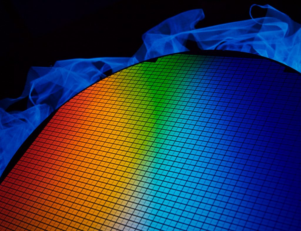
One of the most interesting – and essential – components of electronic and optical devices is the semiconductor. These unique materials have properties somewhere between that of a conductor and that of an insulator, allowing them to control electrical currents. Whether it is the microprocessor in your smartphone, solar panels that provide clean renewable energy or MRI scanners that detect the presence and progression of medical conditions, one thing is clear: semiconductors can be found everywhere.
Because of their ubiquity, the way in which semiconducting materials are produced is crucial. How they are manufactured can impact their cost, energy efficiency and reliability of the devices that they go into.
Dr Yasuo Koide of the National Institute for Material Science in Japan has dedicated his extensive career to unlocking the secrets of what makes a good semiconductor, and how we can apply this knowledge to the development of new and exciting technologies. Alongside his colleagues and collaborators, Dr Koide has made breakthroughs in numerous areas within the field of semiconductors, giving rise to a plethora of important discoveries. Now, with his current team at the National Institute for Material Science, he continues to shed light on the intricate world of semiconducting materials.

Perfecting AlGaN Semiconductors
One important application of semiconductors is the light-emitting diode (LED), which emits light when current is passed through it. LEDs are an important source of energy-efficient light for numerous applications, including display technologies and residential lighting. Those familiar with the history of LEDs may already know the troubled past of producing blue light. In combination with other colours, blue light is required to produce white light. This struggle has motivated scientists across the world to dedicate great effort to developing semiconducting materials that can produce bright and consistent blue light.
During his time as a PhD student at Nagoya University, Dr Koide made significant contributions to this field. His research focused on working with aluminium gallium nitride alloys (AlGaN) in order to produce semiconducting materials. Both aluminium nitride and gallium nitride had previously shown promising potential as LED materials that could produce blue light. However, many researchers struggled to control their specific electronic properties.
By creating a material that contained both aluminium nitride and gallium nitride in a specific ratio, Dr Koide and his colleagues enabled far greater control over tuning the semiconductor’s electrical properties. They successfully produced single-crystal AlGaN films, meaning that the entire film was grown as one large crystal. This was done by feeding the gases trimethyl gallium, trimethyl aluminium and ammonia into a reactor, where the resulting alloy was deposited onto a silicon or sapphire surface. Even more importantly, the team found that by adjusting the reaction conditions, it was possible to control the metal composition of the alloy, leading to customisability in the final material.
‘The key to success was two-fold,’ explains Dr Koide. ‘One was the reactor design, which provided the flow of the precursor gases under high-velocity condition, and the other was to use an aluminium nitride buffer layer.’
This research truly revolutionised the field. Ultimately, this set the foundation that led to other members of the team being awarded the Nobel Prize in Physics in 2014, for the very invention that they had set out to create: high-brightness, energy-efficient, blue LEDs.

SiGe Semiconductor Films
Dr Koide’s research wasn’t just restricted to AlGaN-based materials. At the time, silicon-germanium (SiGe) materials were showing great potential as high-quality semiconductors. The different sizes of the silicon and germanium atoms in SiGe semiconductors allow for a high level of customisation.
However, there was still an issue to overcome: achieving thin films of SiGe. This specific type of semiconductor material was notoriously difficult to produce as a very thin film, which would be required for its use in electronic devices. As such, Dr Koide and his team set out to produce this material in a usable form.
During his time at Nagoya University, Dr Koide managed to grow SiGe films that were a single atom thick. He did this using a technique called gas source molecular beam epitaxy, which involves pumping gaseous forms of silicon and germanium into a vacuum at high temperatures. This causes the elements to be deposited onto a silicon surface, allowing the crystal to grow.
Not only did Dr Koide show that extremely thin films of SiGe could be grown; he also demonstrated that by altering the temperature of the reaction, it was possible to influence the ratio of silicon to germanium in the final material. This led to an even higher level of customisation than was expected, creating the potential for a wider range of use in electronic components.
Investigating Wide-Bandgap Semiconductors
Semiconductors are so useful because of their unique properties and their fine tunability. They can be created to a certain specification, depending on their intended use. One property of semiconductors that researchers often focus on is called the ‘bandgap’. The bandgap is a general indicator used to demonstrate the energy required for the semiconductor to perform its job by allowing electric current to flow.
Generally speaking, pure insulating materials have a bandgap that is too large to overcome; thus, they have almost zero electronic properties. Full conductors essentially have no bandgap, meaning that they readily conduct a current without the need to overcome an energy barrier. As such, semiconducting materials with a large bandgap could be viewed as being more on the insulator side of the semiconductor spectrum, while those with a small bandgap are closer to conductors in their properties.
Whilst at Kyoto University, Dr Koide began to research semiconductors with large bandgaps – so-called ‘wide-bandgap semiconductors’. He began by investigating what happens when he created a semiconductor by combining metal and diamond surfaces, to learn more about the electrical properties of this type of material. In this situation, the difference in the materials creates a semiconducting effect at the interface.
In his study, Dr Koide was able to determine how the electrons, which form electric currents, were able to move between contact points on the metal and diamond materials. This was an important breakthrough, which paved the way for future work involving these unique types of materials. Dr Koide’s work led to numerous discoveries in wide-bandgap semiconductors, such as low-resistance zinc-selenium materials, which have found use due to their high thermal stability, and gallium-based materials that have found uses in blue LEDs.
Diamond-Based Electronic Devices
In many industries, diamond-based materials have always been a tantalising prospect. Their unique structure, comprising a rigid network of carbon atoms, gives them incredible strength and stability, making them useful in a wide variety of potential applications.
‘Diamond is an extreme semiconductor with the strongest mechanical hardness, the largest thermal conductivity, and the highest thermal and chemical stability,’ says Dr Koide. ‘It is highly attractive for applications in electronic and optical devices.’
However, diamond’s unique properties can also lead to some complications. In particular, the incredibly high stability of diamond-based materials can also mean that they have extremely high ‘ionisation energies’. This means that a lot of energy is required to move the electrons within diamond between energy states. This makes diamond less practical as other semiconductors due to this high energy barrier. Scientists rarely give up so easily though, as Dr Koide and his colleagues were keen to prove.
They set out to find real applications for diamond-based semiconductors that would allow these materials to operate at room temperature. One of the team’s major breakthroughs was designing a diamond-based sensor that could detect deep-ultraviolet light, and successfully distinguish it from visible light. These types of sensors are useful for a wide variety of applications, ranging from flame detection to communication between satellites. Historically, it has been a challenge to make sensors that are stable enough to withstand continued exposure to high-energy ultraviolet light. As such, very stable diamond-based sensors provided an ingenious solution to this problem.
In another research project, Dr Koide and his colleagues successfully developed diamond-based transistors. Transistors are the basic building blocks of semiconductor microprocessor chips, with many of the latest-generation chips featuring billions of transistors. However, the vast majority of these microprocessors are based on silicon, which faces significant limitations under certain conditions. For example, silicon-based microprocessors are prone to failure within extremely high-power electronic devices and in harsh environments such as engines or outer-space.
‘Not only are diamond materials physically hard,’ says Dr Koide. ‘They also conduct heat well which means that they can cope with high levels of power and operate in hotter temperatures. In addition, they can endure larger voltages than existing semiconductor materials before breaking down.’ His team’s new transistors are composed of diamond that has been coated with an insulator with a high-dielectric constant – itself a very durable material with high thermal insulation.
‘Ultimately, our team’s goal is to build integrated circuits with diamonds,’ concludes Dr Koide. ‘With this in mind, we hope our work can support the development of energy-efficient devices that can function in conditions of extreme heat or radiation.’
SHARE
DOWNLOAD E-BOOK
LISTEN TO THE AUDIO
REFERENCE
https://doi.org/10.33548/SCIENTIA759
MEET THE RESEARCHER
Dr Yasuo Koide
Research Center for Functional Materials
National Institute for Materials Science (NIMS)
Ibaraki
Japan
Dr Yasuo Koide earned his PhD in electrical engineering from Nagoya University, Japan, in 1987, where he stayed on as a Research Associate and Associate Professor. He then moved to Kyoto University, Japan, where he worked as an Associate Professor until 2002, before starting work at the National Institute for Materials Science (NIMS) in Ibaraki, Japan. Here, he acts as director for the Center for Nanotechnology Platform and Group Leader for the Next-Generation Semiconductor Group in the Research Center for Functional Materials. His research covers many aspects of the design and applications of different semiconductor materials, earning Dr Koide the title of Fellow of the Japanese Society of Applied Physics, as well as the 22nd Masumoto Hakaru award from the Japan Institute of Metals and Materials.
CONTACT
E: koide.Yasuo@nims.go.jp
W: https://samurai.nims.go.jp/profiles/koide_yasuo
KEY COLLABORATORS
Dr Jiangwei Liu, NIMS, Japan
Dr Meiyong Liao, NIMS, Japan
Dr Masataka Imura, NIMS, Japan
Professor Isamu Akasaki, Nagoya University, Japan
Professor Hiroshi Amano, Nagoya University, Japan
Professor Yukio Yasuda, Nagoya University, Japan
Professor Shigeaki Zaima, Nagoya University, Japan
Professor Masanori Murakami, Kyoto University, Japan
FURTHER READING
JW Liu, H Oosato, MY Liao, Y Koide, Enhancement-mode hydrogenated diamond metal-oxide-semiconductor field-effect transistors with Y2O3 oxide insulator grown by electron beam evaporator, Applied Physics Letters, 2017, 110, 20, 203502.
JW Liu, MY Liao, M Imura, A Tanaka, H Iwai, Y Koide, Low on-resistance diamond field effect transistor with high-k ZrO2 as dielectric, Scientific Reports, 2014, 4, 6395.
MY Liao, S Hishita, E Watanabe, S Koizumi, Y Koide, Suspended single-crystal diamond nanowires for high-performance nanoelectromechanical switches, Advanced Materials, 2010, 22, 5393.
MY Liao, Y Koide, High-performance metal-semiconductor-metal deep-ultraviolet photodetectors based on homoepitaxial diamond thin film, 2006, Applied Physics Letters, 2006, 89, 113509.
Y Koide, T Maeda, T Kawakami, S Fujita, T Uemura, N Shibata, M Murakami, Effects of annealing in an oxygen ambient on electrical properties of Ohmic contacts to p-GaN, Journal of Electronic Materials, 1999, 28, 3, 341.
M Yokoba, Y Koide, A Otsuki, A Ako, T Oku, M Murakami, Carrier transport mechanism of Ohmic contact to p-type diamond, Journal of Applied Physics, 1997, 81, 10, 6815.
Y Yasuda, Y Koide, A Furukawa, N Ohshima, S Zaima, Relationship Between Growth Processes and Strain Relaxation in Si1-xGex Films Grown on (100)Si-(2×1) by Gas Source Molecular Beam Epitaxy, Journal of Applied Physics, 1993, 73, 5, 2288.
Y Koide, H Itoh, MRH Khan, K Hiramatsu, N Sawaki, I Akasaki, Energy Band-gap Bowing Parameter in An AlxGa1-xN Alloy, Journal of Applied Physics, 1987, 61, 9, 4540.
Y Koide, H Itoh, N Sawaki, I Akasaki, M.Hashimoto, Epitaxial Growth and Properties of AlxGa1-xN by MOVPE, Journal of the Electrochemical Society, 1986, 133, 9, 1956.
![]()
REPUBLISH OUR ARTICLES
We encourage all formats of sharing and republishing of our articles. Whether you want to host on your website, publication or blog, we welcome this. Find out more
Creative Commons Licence (CC BY 4.0)
This work is licensed under a Creative Commons Attribution 4.0 International License. 
What does this mean?
Share: You can copy and redistribute the material in any medium or format
Adapt: You can change, and build upon the material for any purpose, even commercially.
Credit: You must give appropriate credit, provide a link to the license, and indicate if changes were made.
SUBSCRIBE NOW
Follow Us
MORE ARTICLES YOU MAY LIKE

Dr Olalla Castro-Alvaredo | Measuring Entanglement: Symmetry-Resolved Entropy
Dr Olalla Castro-Alvaredo of the City University of London (UK) and her collaborators are advancing our understanding of an important phenomenon of quantum mechanical systems known as entanglement and, especially, its mathematical measures. Symmetry-resolved entanglement entropy is one such measure. Their study focuses on special quantum states which are excited with respect to a ground state. The research shows how the entanglement amongst quantum particles can be measured and assesses the contribution to the entanglement of quasiparticle excitations, particularly in the presence of additional symmetries.
Dr Tsun-Kong Sham – Dr Jiatang Chen – Dr Zou Finfrock – Dr Zhiqiang Wang | X-Rays Shine Light on Fuel Cell Catalysts
Understanding the electronic behaviour of fuel cell catalysts can be difficult using standard experimental techniques, although this knowledge is critical to their fine-tuning and optimisation. Dr Jiatang Chen at the University of Western Ontario works with colleagues to use the cutting-edge valence-to-core X-ray emission spectroscopy method to determine the precise electronic effects of altering the amounts of platinum and nickel in platinum-nickel catalysts used in fuel cells. Their research demonstrates the potential application of this technique to analysing battery materials, catalysts, and even cancer drug molecules.

Dr Marcus Noack and Dr Mark Risser | Advancing Gaussian Processes: The Noack-Risser Method
Dr Marcus Noack and Dr Mark Risser, researchers at Lawrence Berkeley National Laboratory, have recently proposed a significant advancement in the area of machine learning and data science that promises significant computational improvements: the enhancement of exact Gaussian Processes for large datasets, significantly improving data analysis capabilities for samples even beyond 5 million data points.
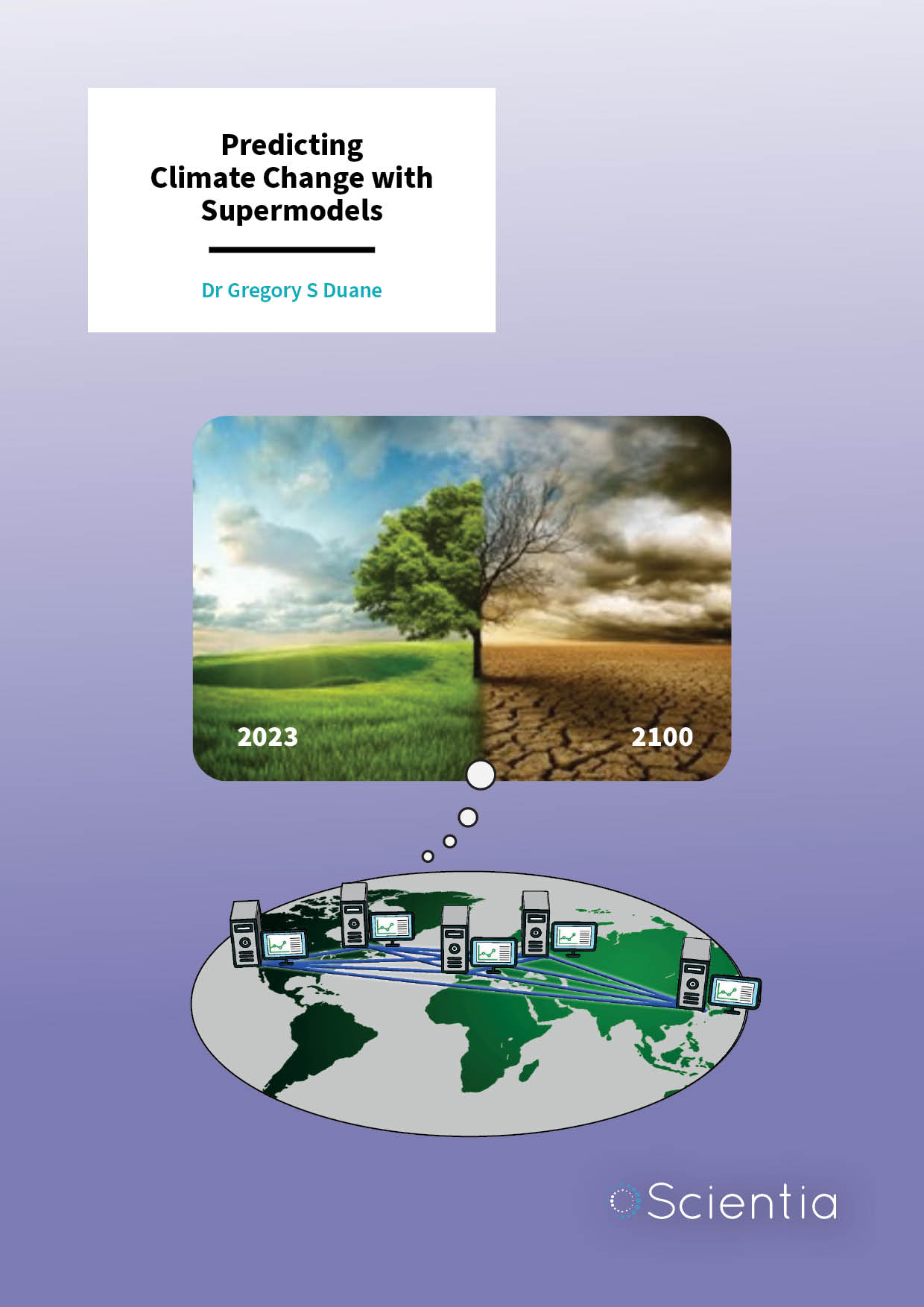
Dr Gregory Duane | Predicting Climate Change with Supermodels
Our universe is comprised of fascinatingly complex systems. Systems such as the Earth’s climate can, at first glance, seem far too complex and chaotic to predict accurately. Dr Gregory Duane and his team at the University of Colorado have been developing complex computational models that can learn from past data, providing us with intriguing insights and more accurate predictions about the future.